Quantum Computers Built with Traditional Silicon Technology
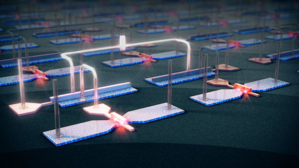
Modern micro-processors and memory devices contain billions of transistors on a chip, yet all of these transistors are controlled only by a small number of input-output ports. Future quantum computers may have to follow the same path because large numbers of quantum bits (qubit) will be required to perform complex tasks. By using quantum dot (QD) devices that have been fabricated alongside classical nanowire field-effect-transistors (FET) on a silicon chip, in a recent paper that appeared in Nature Electronics, a team including Chancellor's Fellow Dr Alessandro Rossi applied these concepts to quantum information processing at milliKelvin temperatures.
An efficient way to readout a single qubit device is by using signals that are close to the frequency at which radios operate, and by coupling the quantum device to a careful engineered resonant circuit. However, one resonator per qubit is not a scalable approach. So we borrowed concepts for addressing and charge storage found in Dynamic Random Access Memory (RAM). We connected our readout resonator to the channel of a single wide-body FET, via bond wires, which then conditionally passes the signal on to the gate of a short channel transistor device, via another bond wire, in which the QDs are formed. We found that the control FET still operates well at milliKelvin and we achieved conditional readout at a sensitivity comparable to direct measurements. Additionally, we observed single electron storage on the QD of the order of 1 second when the FET is operated in the off state. We then duplicated this circuit and realised a 2-cell RAM to address two QDs. In this configuration, we were able to show sequential readout of two devices, which is the basis for dynamic random access of many cells.
Finally, we wanted to better understand why our circuit performed well in order to give guidelines for future designs of integrated classical-quantum circuits. We therefore looked more closely into control FETs of different sizes, which were available on the same chip, and develop a model of the resistance and capacitance depending on channel width and gate length. Using a readout model, we evaluate the readout signal-to-noise ratio as a function of these scaling parameters and find that the choice we made at the beginning, of using a FET of large channel width and small gate length, was the right choice, as the low resistance of a wide channel device maximises the SNR. However, to allow readout of a large scale device efficiently the size of the FET needs to be scaled down. Our models show that the FET width can be scaled by a factor of 100 allowing dense integration while maintaining sufficient SNR by compromising on retention time and voltage noise.
More background information is also available at The Conversation.
September 2019