Range of AnalysesMicrostructural analysis
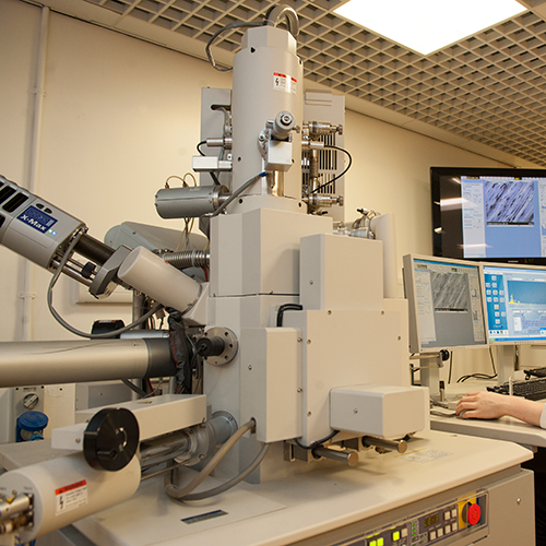
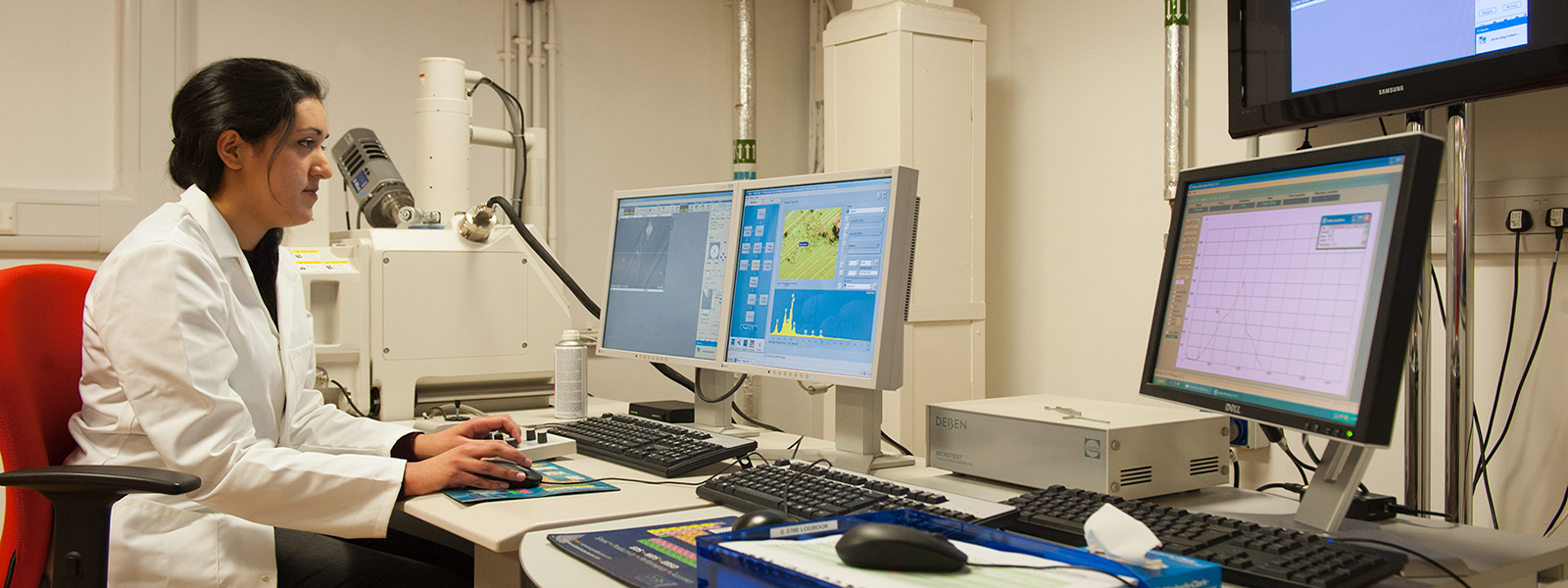
Scanning Electron Microscopes (SEM)
With the HITACHI S-3700N tungsten filament SEM and the HITACHI SU-6600 high-resolution field emission FE-SEM, we can perform a variety of analyses:
- Morphological and topographical imaging
- Surface fractography
- Materials microstructure
- Grain size and texture analysis by electron backscattered diffraction (EBSD)
- Scanning transmission electron microscopy (STEM) on thin films
- Variable pressure mode for non-conductive specimens – i.e. no need for carbon/gold coat
- Non-destructive analysis on small components through a large chamber (300 x 110mm)
- In-situ micro-mechanical tests (2kN load cell and video capture)
- Environmental capability.
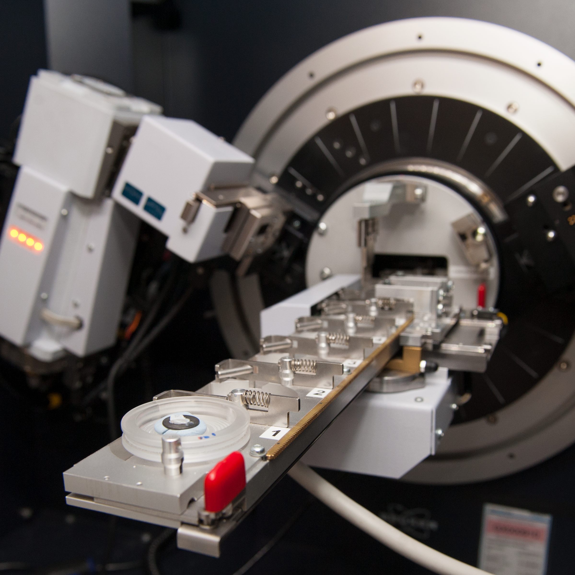
X-Ray Diffractometer (XRD)
- The BRUKER D8 ADVANCE with DAVINCI XRD extracts structural information material and phase identification from metals and ceramics
- Analysis can be completed at ambient and elevated temperatures up to 2000oC
- Specimens can be in bulk or powder form, thin films, corrosion products or debris
- Measured properties include phase composition, crystal structure, lattice parameters and mismatches, spatial orientation of crystals, crystallinity, residual stress, grain texture, and layer thickness.
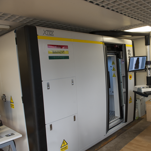
X-ray Computed Tomography Scanner
- The Nikon XT H 225 LC non-destructively produces high-resolution (1.5μm) volume images of any material based on density contrasts
- Measures porosity and permeability characterisation, deformation in a solid medium, phase characterisation and in-situ feature measurement
- Liquid or dry environment
- Deben CT 10kN cell for specimens imaging in real time under controllable environmental conditions
- 225kV X-ray source of reflection and transmission.

Optical Microscopy (OM)
- The Olympus GX51 inverted microscope suitable for observations of metallographic specimens
- Wide variety of observation methods including brightfield, darkfield, differential interference contrast, polarisation
- Magnification range from x50 to x1000
- Image capture with a 3Mp digital camera.

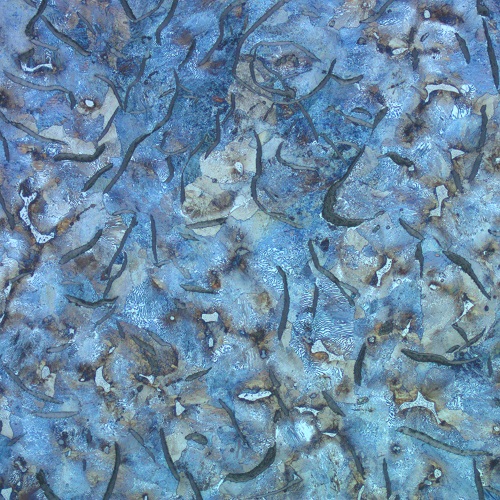
SEM scan showing brittle intergranular fracture

Complete 3D XCT scan of cement
Optical micrograph using polarised light to show etched pearlitic grey iron