Coordinated with the Colloquia at the Department of Physics and Astronomy of the University of Glasgow. (They may have donuts but we have free chocolate covered biscuits and coffee!)
Colloquia Schedule 2023-2024
* Note: Outside of regular schedule.
Coordinated with the Colloquia at the Department of Physics and Astronomy of the University of Glasgow. (They may have donuts but we have free chocolate covered biscuits and coffee!)
* Note: Outside of regular schedule.
Prof K Long (Physics, ICL) and Prof A Giaccia (Oncology, Oxford) - 3pm, TL328
Cancer is the second most common cause of death globally. In 2018, 18.1 million new cancer cases were diagnosed, 9.6 million people died of cancer-related disease, and 43.8 million people were living with cancer. Radiotherapy (RT) is used in 50% of cancer patients and is involved in 40% of cancer cures. It is estimated that 26.9 million life-years could be saved in low- and middle-income countries if capacity could be scaled up.
The beam characteristics that can be exploited in proton- and ion-beam therapy (IBT) facilities today are restricted to low dose rates, a small number of temporal schemes, and a small number of spatial distributions. The use of novel beams with strikingly different characteristics has led to exciting evidence of enhanced therapeutic benefit. This evidence, together with developments in our understanding of personalised medicine based on the biology of individual tumours, now provides the impetus for a radical transformation of IBT.
The ‘Laser-hybrid Accelerator for Radiobiological Applications’, LhARA, is conceived as a novel, uniquely flexible facility dedicated to the study of radiobiology. The technologies that will be demonstrated in LhARA have the potential to allow particle-beam therapy to be delivered in a completely new regime, combining a variety of ion species in a single treatment fraction and exploiting ultra-high dose rates. The laser-hybrid approach will allow the exploration of the vast “terra incognita” of the mechanisms by which the biological response is modulated by the physical characteristics of the beam. We will describe the motivation for LhARA, present the status of its development and summarise the programme upon which the LhARA consortium has embarked to drive a step-change in clinical capability.
Dr Anton Idlerton (University of Edinburgh) 25th October 2023, 3pm, TL328

High-intensity lasers offer new opportunities for probing fundamental physics, in particular quantum electrodynamics, in a regime rarely tested in experiment. Among the target processes for future experiments are “vacuum birefringence”, in which the vacuum, exposed to intense light, behaves much like a birefringent medium, and “pair production”, the creation of matter from light. In this talk I will give an introduction to the theory behind vacuum birefringence, as well as both direct and indirect approaches to its measurement, the latter via direct measurements of pair production and invoking unitarity in the form of Kramers-Kronig relations.
Prof Rachel Oliver (University of Cambridge) 21st February 2024, JA 314
Porous semiconducting nitrides are effectively a new class of semiconducting material, with properties distinct from the monolithic nitride layers from which devices from light emitting diodes (LEDs) to high electron mobility transistors are increasingly made. The introduction of porosity provides new opportunities to engineer a range of properties including refractive index, thermal and electrical conductivity, stiffness and piezoelectricity. Quantum structures may be created within porous architectures and novel composites may be created via the infiltration of other materials into porous nitride frameworks.
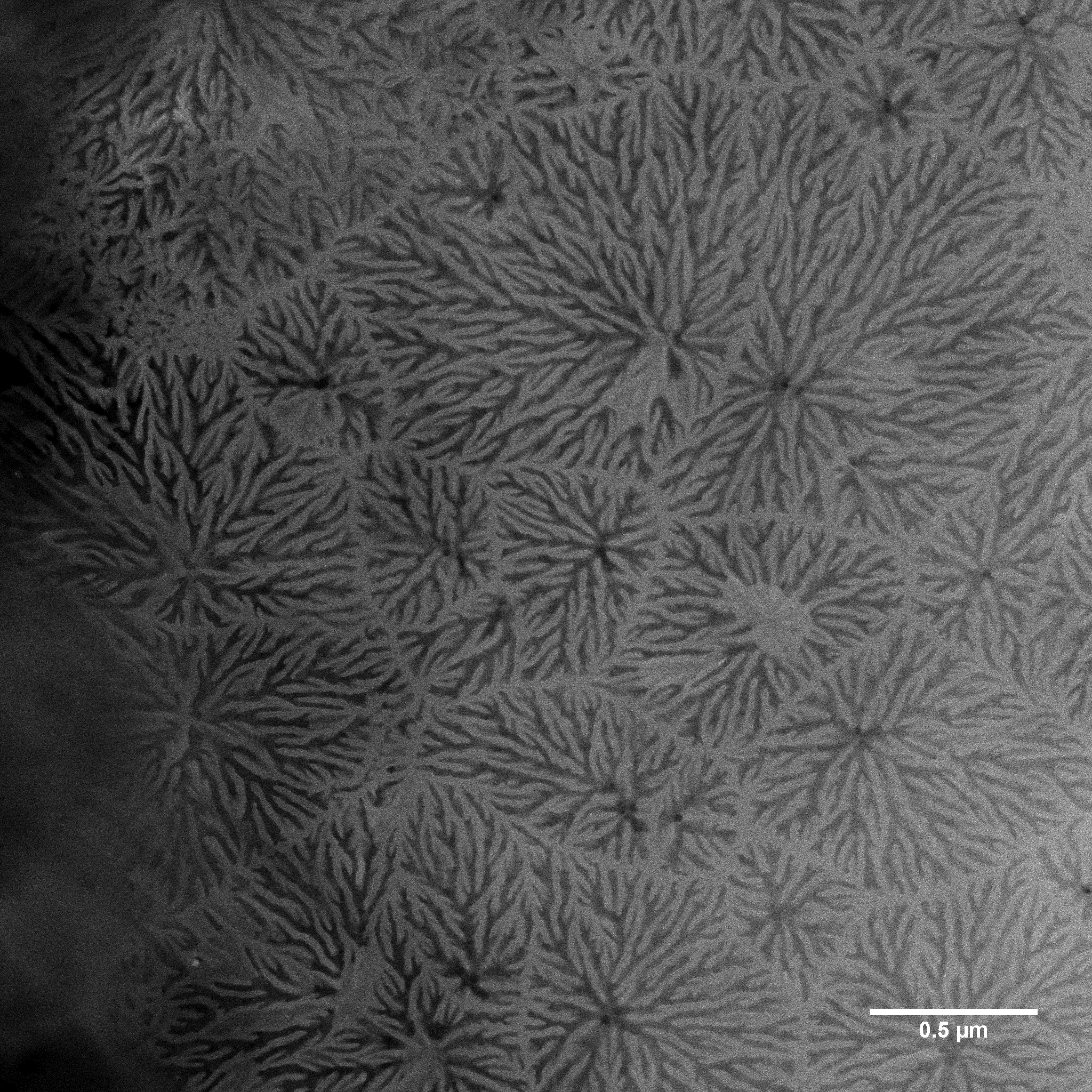
Scanning transmission electron microscopy image of a single sub-surface porous layer, which the etchant has accessed via defect related channels.
A key example of the application of porous nitrides in photonics is the fabrication of high reflectivity distributed Bragg reflectors (DBRs) from alternating layers of porous and non-porous GaN. These reflectors are fabricated from epitaxial structures consisting of alternating doped and undoped layers, in which only the conductive, doped layers are electrochemically etched. Conventionally, trenches are formed using a dry-etching process, penetrating through the multilayer, and the electrochemical etch then proceeds laterally from the trench sidewalls. The need for these trenches then limits the device designs and manufacturing processes within which the resulting reflectors can be used. We have developed a novel alternative etching process, which removes the requirement for the dry-etched trenches, with etching proceeding vertically from the top surface through channels formed at naturally-occurring defects in the crystal structure of GaN (see Figure). This etch process leaves an undoped top surface layer almost unaltered and suitable for further epitaxy.
This new defect-based etching process provides great flexibility for the creation of a variety of sub-surface porous architectures on top of which a range of devices may be grown. Whilst DBR structures enable improved light extraction from LEDs and the formation of resonant cavities for lasers and single photon sources, recent development also suggests that thick, sub-surface porous layers may enable strain relaxation to help improve the efficiency of red microLEDs for augmented reality displays. Meanwhile, the option of filling pores in nitride layers with other materials provides new opportunities for the integration of nitrides with emerging photonic materials, such as the hybrid-perovskite semiconductors, with perovskites encapsulated in porous nitride layers demonstrating greatly improved robustness against environmental degradation.
Prof Bengt Eliasson (University of Strathclyde), 6th March 2024, JA 314
In this talk I will present a few of my research areas on the interaction between electromagnetic waves and plasmas, employing different numerical simulations approaches. Since plasmas contain a large number of charged particles (electrons, ions) they can support their own electrostatic and electromagnetic fields and waves, and the interaction with electromagnetic waves is very rich and can occur on different time and length scales. When the plasma is permeated by a magnetic field, the existing waves are modified and many new wave modes with unique characteristics can appear in the plasma. I will discuss multi-scale phenomena taking place in both space physics using radio waves, in laboratory plasma using microwaves, and Laser-plasma interaction where the effects of thermal emissions (one of many applications of the ‘fluctuation-dissipation theorem’) can be important. I will discuss both fluid and kinetic simulations and how they may complement each other for different cases.
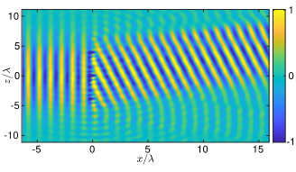
Janne Ruostekoski (Lancaster University) 20th March 2024, JA 314
Light can mediate strong coupling between resonant emitters in dense and homogeneous ensembles. Even in classical systems the response can become cooperative in which case the wave is repeatedly scattered by the same emitters, resulting in a correlated optical response and dramatic violation of standard textbook optics. The strong cooperative response can be harnessed by confining cold atoms in regular planar arrays, formed, for instance, by optical lattices. In such systems, the light can be manipulated and structured, and the coupled system of atoms and light can exhibit strongly correlated quantum phenomena.